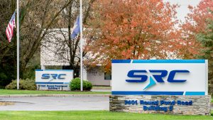
VESTAL, N.Y. — Binghamton University will use a federal funding award of $1 million to purchase advanced–packaging equipment for its nanofabrication laboratory (NLAB).
The funding award seeks to “bolster” workforce training for advanced chip manufacturing in cleanroom environments.
The funding is part of the fiscal year 2024 appropriations bills as a congressionally directed spending request, U.S. Senate Majority Leader Charles Schumer (D–N.Y.) and U.S. Senator Kirsten Gillibrand (D–N.Y.) announced on April 2.

Cybersecurity in Today’s Remote Work Environment
The response to the COVID-19 pandemic demonstrated that remote work was viable for many companies. Today, remote and hybrid work models have become standard options for most professionals. While remote

Recent Court Decision Supports Requiring Employees to Be In the Workplace
A recent Federal Court decision confirmed that the Family Medical Leave Act (FMLA) does not require employers to allow employees to work remotely. In Kemp v. Regeneron Pharmaceuticals, Inc.,
The federal investment will help get students the skills they need for “in-demand”careers in the semiconductor industry “being spurred by Schumer’s CHIPS & Science Law,” Schumer’s office said.
“I am proud to deliver this $1 million federal investment to Binghamton University to supercharge the Southern Tier’s semiconductor workforce training with new state-of-the-art equipment that will help replicate real cleanrooms at chip companies,” Schumer saidin the announcement. “Together with fantastic institutions like Binghamton University leading the way, we are ensuring the next generation of engineers, scientists, and innovators are trained and work here in Upstate NY.”
The senators said the purchase of new, advanced–packaging equipment will allow electronics with sub-micron circuitry to be fabricated, analyzed, and tested by participants from across industry and academia.
The equipment will provide students with hands-on training to prepare them for careers in semiconductor manufacturing.
The lab’s participants will be trained in next-generation electronics, including 2.5D and 3D chip packaging, “developing a pipeline of qualified talent” to support the growth of the advanced electronics manufacturing and packaging industry across upstate New York, Schumer’s office said.